*PI2115,Pololu原廠 5V 升壓模組(U3V12F5)Step-Up Voltage Regulator

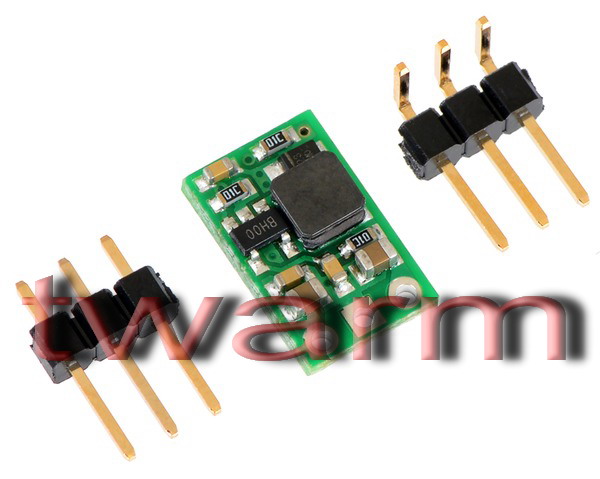
The compact (0.32"×0.515") U3V12F5 switching step-up (or boost) voltage regulator takes an input voltage as low as 2.5 V and efficiently boosts it to 5 V. The pins have a 0.1" spacing, making this board compatible with standard solderless breadboards and perfboards.
緊湊型 (0.32“×0.515”) U3V12F5 開關升壓(或升壓)穩壓器可承受低至 2.5 V 的輸入電壓,並可有效升壓至5 V。引腳間距為 0.1“ 使該板與標準無焊試驗板和穿孔板相容。
| 一般規格 | 最低工作電壓: | 2.5 V | | 最大工作電壓: | 5 V | | 最大輸入電流: | 1.4 安培2 | | 輸出電壓: | 5 V | | 反向電壓保護? | N | | 最大靜態電流: | 2毫安
| |  |
我們建議將U1V10F5 或U1V11F5作為具有更寬工作電壓範圍和類似輸出電流能力的替代品。

【Overview】
These boost (step-up) voltage regulators generate higher output voltages from input voltages as low as 2.5 V. They are switching regulators (also called switched-mode power supplies (SMPS) or DC-to-DC converters) and have a typical efficiency between 80% to 90%. The available output current is a function of the input voltage, output voltage, and efficiency (see Typical Efficiency and Output Current section below), but the input current can typically be as high as 1.4 A. This regulator is available with a fixed 5 V, 9 V, or 12 V output:
這些升壓(升壓)穩壓器從低至 2.5 V 的輸入電壓產生更高的輸出電壓。它們是開關穩壓器(也稱為開關模式電源 (SMPS) 或 DC-DC 轉換器),典型效率在 80% 至 90% 之間。
*可用輸出電流是輸入電壓、輸出電壓和效率的函數(參見下面的典型效率和輸出電流部分),但輸入電流通常可高達1.4 A。
*該穩壓器提供固定的5V、9V或12V輸出:
The regulator’s thermal shutdown prevents damage from overheating, but it does not have short-circuit or reverse-voltage protection.
We have several other boost regulators that you might consider as alternatives to these:
- 3.3V or 5V boost regulator NCP1402 – lower-current alternatives that work with input voltages as low as 0.8 V.
- Adjustable boost regulator 2.5-9.5 V – output voltage is adjustable from 2.5 to 9.5 V; works with input voltage as low as 1.5 V.
- Adjustable boost regulator 4-25 V – output voltage is adjustable from 4 to 25 V; works with input voltage as low as 1.5 V.
【Features】
- input voltage: 2.5 V – VOUT
- fixed 5 V, 9 V, or 12 V output with 4% accuracy
- 1.4 A switch allows for input currents up to 1.4 A
- 2 mA typical no-load quiescent current
- integrated over-temperature shutoff
- small size: 0.515" × 0.32" × 0.1" (13 × 8 × 3 mm)
特徵
- 輸入電壓:2.5 V – VOUT
- 固定 5 V、9 V 或 12 V 輸出,精度為 4%
- 1.4 A 開關允許高達 1.4 A 的輸入電流
- 2 mA 典型空載靜態電流
- 集成過溫關斷
- 小尺寸:0.515“ × 0.32” × 0.1“(13 × 8 × 3 mm)
〔Using the Regulator〕
Connections
The boost regulator has three connections: input voltage (VIN), ground (GND), and output voltage (VOUT).升壓穩壓器有三個連接:輸入電壓 (VIN)、接地 (GND) 和輸出電壓 (VOUT)。
The input voltage, VIN, must be at least 2.5 V and should not exceed the output voltage, VOUT. Please be wary of destructive LC spikes that might cause the input voltage to exceed VOUT (see below for more information).
輸入電壓 VIN 必須至少為 2.5 V,且不應超過輸出電壓 VOUT。請注意可能導致輸入電壓超過VOUT的破壞性LC尖峰(有關更多資訊,請參見下文)。
The three connections are labeled on the back side of the PCB, and they are arranged with a 0.1" spacing along the edge of the board for compatibility with solderless breadboards, connectors, and other prototyping arrangements that use a 0.1" grid. You can solder wires directly to the board or solder in either the 3×1 straight male header strip or the 3×1 right-angle male header strip that is included.
〔Typical Efficiency and Output Current〕
The efficiency of a voltage regulator, defined as (Power out)/(Power in), is an important measure of its performance, especially when battery life or heat are concerns. As shown in the graphs below, this switching regulator typically has an efficiency of 80 to 90%.
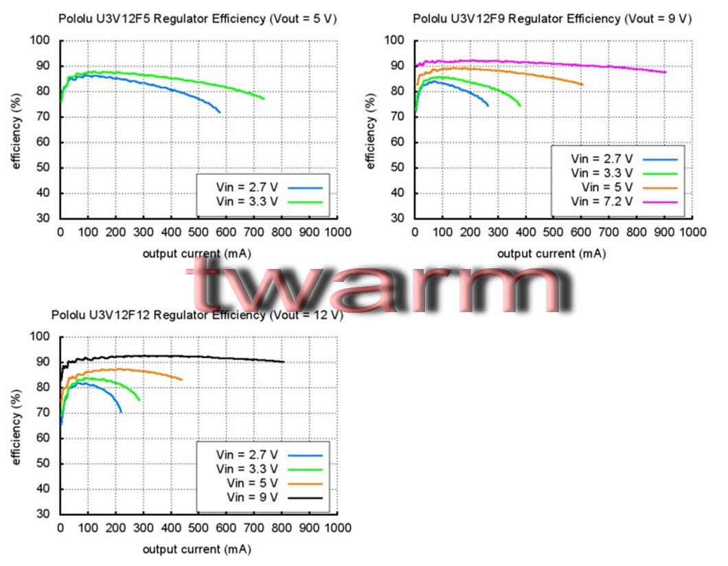
The maximum achievable output current is approximately proportional to the ratio of the input voltage to the output voltage. If the input current exceeds the switch current limit (typically somewhere between 1.4 and 2 A), the output voltage will begin to drop. Additionally, the maximum output current can depend on other factors, including the ambient temperature, air flow, and heat sinking.
〔LC Voltage Spikes〕
When connecting voltage to electronic circuits, the initial rush of current can cause damaging voltage spikes that are much higher than the input voltage. In our tests with typical power leads (~30" test clips), input voltages above 10 V caused voltage spikes in excess of 20 V. You can suppress such spikes by soldering a 33μF or larger electrolytic capacitor close to the regulator between VIN and GND.
More information about LC spikes can be found in our application note, Understanding Destructive LC Voltage Spikes.


